TSMC Unveils A14 Node to Boost AI Performance
Taiwan Semiconductor Manufacturing Company (TSMC) has announced its latest world-leading process technology, A14, designed to drive significant advances in AI data centers while substantially improving their power efficiency. Compared to TSMC’s current industry-leading N2 process that is set to enter production later this year, A14 promises to improve speed by up to 15% at the same power consumption or reduce power by as much as 30% at the same speed. Additionally, the new process will achieve a more than 20% increase in logic density.
Key Features of A14 Process
TSMC plans to begin manufacturing chips for major AI customers like Nvidia using the A14 process in 2028. “TSMC’s cutting-edge logic technologies like A14 are part of a comprehensive suite of solutions that connect the physical and digital worlds to unleash our customers’ innovation for advancing the AI future,” stated TSMC CEO C.C. Wei in a prepared statement.
The company has been caught off guard by the surging demand for AI chips, according to TSMC senior VP Kevin Zhang. “We thought that edge devices, smartphones, and IoT combined should be the largest consumers of advanced silicon, but no more, largely because of AI. The surge of AI really has substantially changed the landscape of the semiconductor industry,” Zhang explained.

Powering Future Devices
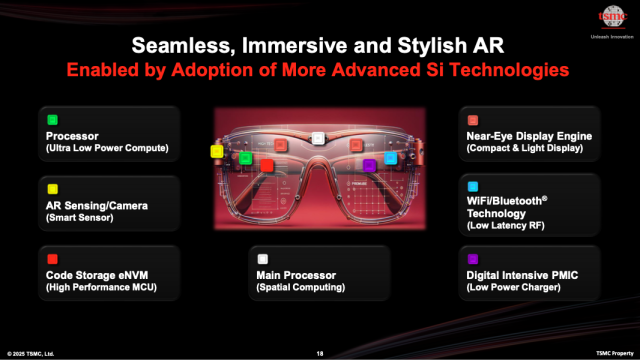
TSMC described how the A14 process could enable the development of new devices such as smart glasses, which could potentially overtake smartphones as the largest consumer electronics device by shipments. “For a full day of battery usage in smart glasses, advanced silicon will require a lot of sensors and connectivity,” Zhang noted. “In terms of silicon content, this can rival a smartphone going forward.”
Advancements in Silicon Photonics
To support the rollout of the A14 node, TSMC is developing silicon photonics technology, which uses light to speed processing in data centers while reducing power consumption. “We think that today’s test substrate technology is capable of bringing integration together between a compute tile and the optical engine,” Zhang said. This technology is expected to replace copper interconnects with silicon photonics, significantly reducing power consumption.

Future Developments
TSMC’s A14 will not initially feature backside power delivery, a technology recently introduced by Intel. However, the company plans to introduce a derivative version of A14 with its own backside power scheme, dubbed Super Power Rail, in 2029. TSMC will use this backside power scheme for the first time with its N16 node in the second half of 2026.

Challenges in Chip Design
As chip designs become increasingly large, exceeding the 850 mm2 size of a reticle, TSMC is developing silicon-on-wafer technology. “You use a wafer to build interposer, then you put all the die on top of it,” Zhang explained. “This effectively gives you 40× the reticle size, the capability in terms of integration, bringing logic and high-bandwidth memory together.”

Lithography Developments
Surprisingly, TSMC does not currently plan to use high-NA EUV lithography tools from ASML for chips ranging from the 2-nm node to the A14 node. “From 2 nanometers to A14, for example, we don’t have to use high-NA but we can continue to maintain similar complexity in terms of processing steps,” Zhang said.
TSMC’s advancements in process technology are positioning the company at the forefront of AI chip manufacturing, with significant improvements in performance and power efficiency. As the demand for AI continues to grow, TSMC’s A14 node is set to play a crucial role in powering the next generation of AI data centers and devices.


